SkyFax: A new dial-up modem that fits in your pocket
Alternative title: "I just wanted to hear some funky sounds..."
Let's talk about another project I did that I've been meaning to write about for a while...
So a bit ago, I was working on an electronic badge. That badge never got finished, but one of its cool features was going to be that it can connect to a phone line and send/receive faxes. I didn't want to re-do the entire board and re-route every trace every time there was a change with the modem, so it became its own separate board, and now a separate mini-project.
I've realized while writing this that it reads a bit like a rough guide to PCB design, rather than just focusing on this specific project's goals and design ideas.
Component Selection
To start, I started looking around for other projects, circuits, and reference schematics. I knew I wanted a V.92, the classic 56k modem. There were a handful of resources for setting up dial-up or faxes (and technical details on how they work), but I could not find too much information on building the modem itself. I figured that they are usually pretty complicated to implement raw and usually done on a dedicated chip, mixing in digital and analog circuitry. And since I like to make most of my projects open-source, I wanted to find a chip that was readily available for most hobbyists, so:
- Not pulled out from another existing modem
- Don't need to sign NDAs for access to part + documents
- In stock
- Still actively manufactured if possible (at least in 2024)
- Can be obtained in single quantities (or relatively small quantities).
So I just went on DigiKey and started looking for a chip.
Under DigiKey's Product Index -> Integrated Circuits (ICs) -> Interface -> Modems - ICs and Modules, there are actually plenty of products listed.
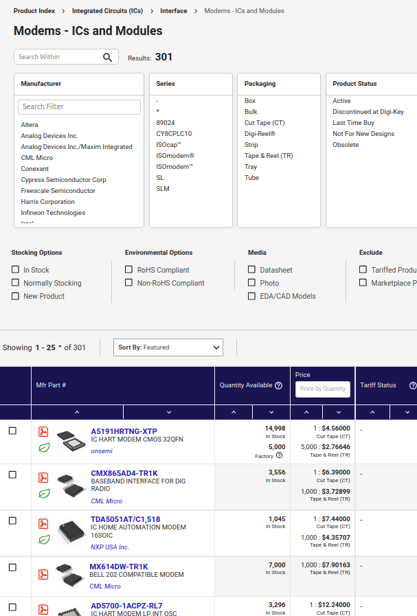
I started adding filters to reduce the matches to in hopes I would find a chip I can use for this project. Firstly, part needs to be in stock (results reduced to ~116). I don't care for any of the other data formats like "Bell 202" or slower ones like V.23 (at least for this project), so selecting filters that included "V.92" reduced the matches greatly, all the way down to 8. I saw one marked "Obsolete", so I selected "Active" in the "Product Status" filter (down to 7).
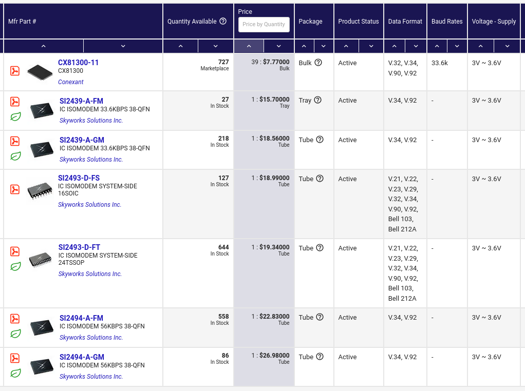
I ignored the first one (the Conexant one) because I didn't want to buy 39 of the chips I wasn't sure if it would work (and I definitely don't need that many).
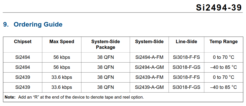
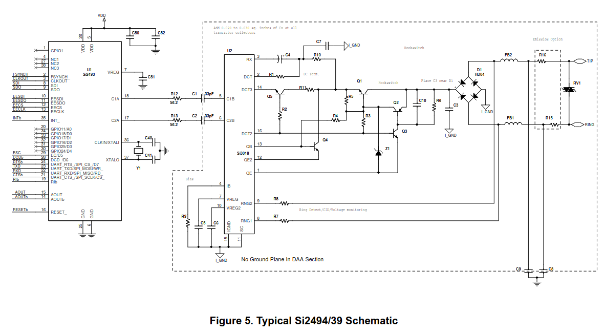
To find our chip, I must now look through the datasheets. From the datasheet1, I found that the Si2494 and Si2439 are basically compatible/interchangeable and the only difference is the max speed.
DigiKey has the compare feature, but it didn't help much between those two, probably because they share the datasheet, and it lists both speeds.
Now, between the Si2494 and the Si2493... I don't remember why, but I went with the 94. (OOGA BOOGA HIGHER NUMBER BETTER maybe?)
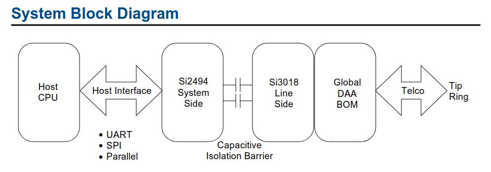
Another thing I can learn from the datasheets is that the Si2494/39 is the "system-side" and there's a complimentary "line-side" component, which is the Si3018.
The typical application schematics' in there too in section 2, followed by the Bill of Materials (component values and part numbers).
You can often find evaluation boards for specific chips or families of chips that use the part and the reference circuit provided. It can help with debugging since there's a known-working board in front of you, as well as developing and testing the software while the hardware is being built. For the Si2494, there's the SI2494-A-FM18-EVB.
Additionally, there may be an Application Note from the manufacturer for designing around a certain component. In our case, we have the AN93 Modem Designers Guide. That document proved invaluable for developing this project. It provides detailed explanations and guides of different components of the chip, for designing the hardware, explanations of AT commands supported, as well as programming examples.
I looked through the datasheet and for its features and interfaces it supports. For this project, this chip was good enough and exactly what I was looking for.
Circuit Design and Schematics
This part is relatively straight-forward, given we have the reference schematics.
System-side
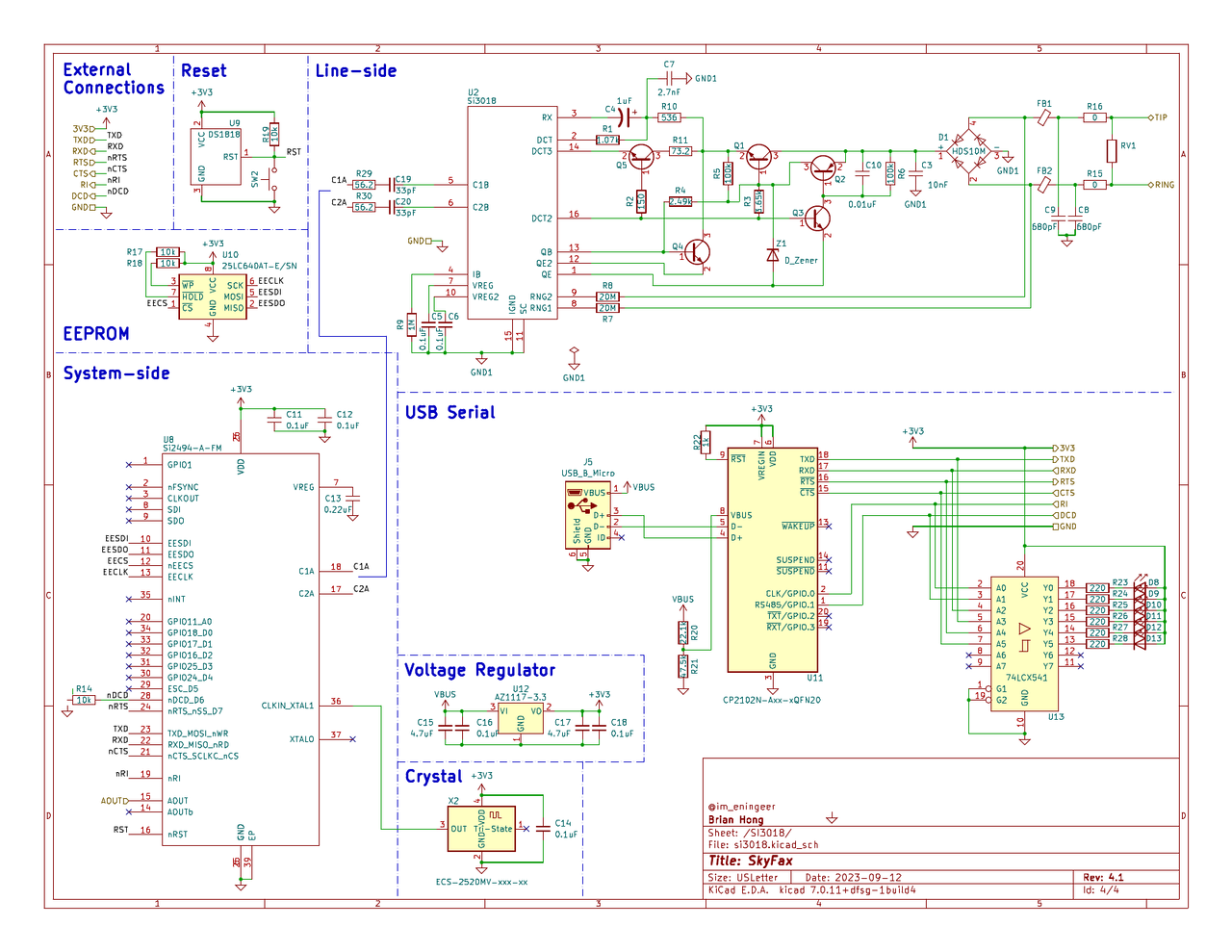
The system-side (computer side) of the schematic is pretty straight-forward, even without the reference schematics.
The Si2494 supports 3 different interfaces for communicating with the host: asynchronous (UART), serial (SPI), and parallel. I chose to use the UART interface becuase it's the simplest (and the default) and I can just slap a USB-to-UART chip on there for a couple cents. I used a Silicon Labs CP2102 for the USB to UART bridge. I also added an LDO2 regulator for powering the 3.3v circuit from the 5v USB, and an EEPROM chip, so that the modem can be programmed if desired.
So it roughly looks like this:
USB Connector -> CP2102 USB-UART bridge -> Si2494 -> (to line side)
                                            v
                                           EEPROM
Line-side
The line-side (telephone side), however, is a bit more complex, utilizing mostly analog components and even some impedance control. Luckily, the AN933 goes over all that, and hopefully just using the reference schematics should get us pretty close enough for things to work properly.
I don't have much else to say for this section besides that I just went through the application note3 and hoped for the best.
KiCAD
I drew it up in KiCad4.
Rough outline of the steps are:
- Add components
- Connect wires
- Label values and designators
KiCAD has a nice little button for auto-filling in reference designators.
For this schematic though, I tried to keep the reference designators the same as the ones provided in the datasheet, to not confuse myself later. - Assign footprint for each component
This is usually where I search and find the actual part as I go through each of the components. Sometimes the exact recommended part is not available and I need to find one that is. Most of the passives should be easy to replace, making good note of the specs required (for resistors, for example: resistance, tolerance, max power). Footprint/size is less important (as long as the part itself would work) since I'll be designing around it anyways, but I try to go for smaller parts.
'Oh, I'll get the smallest parts and fit the entire circuit in X-by-X area! It'll be compact!', says the voice in my head every time. And then I order 0201 sized resistors... It's fine, I've done it, and worked out well, but most of the time, it's unnecessarily small (like, really REALLY small. You can breath wrong and they'll end up on the floor, never to be found again.) Not to mention how annoying it can be to solder them sometimes, especially if everything is all crowded together.
KiCAD should have almost all the standard footprints, as well as for common components, but sometimes I have to get the custom footprint from online or draw them myself.
Another thing I do during this step is to create a new field/property and put the DigiKey part number into it. This makes it very easy to export the BoM (parts list) and upload to DigiKey, where it'll create a list for me with all the components and quantities parsed from it.

PCB Layout
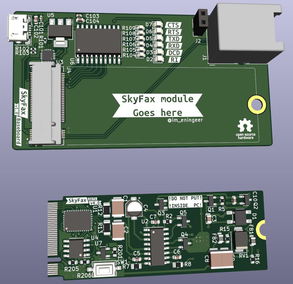
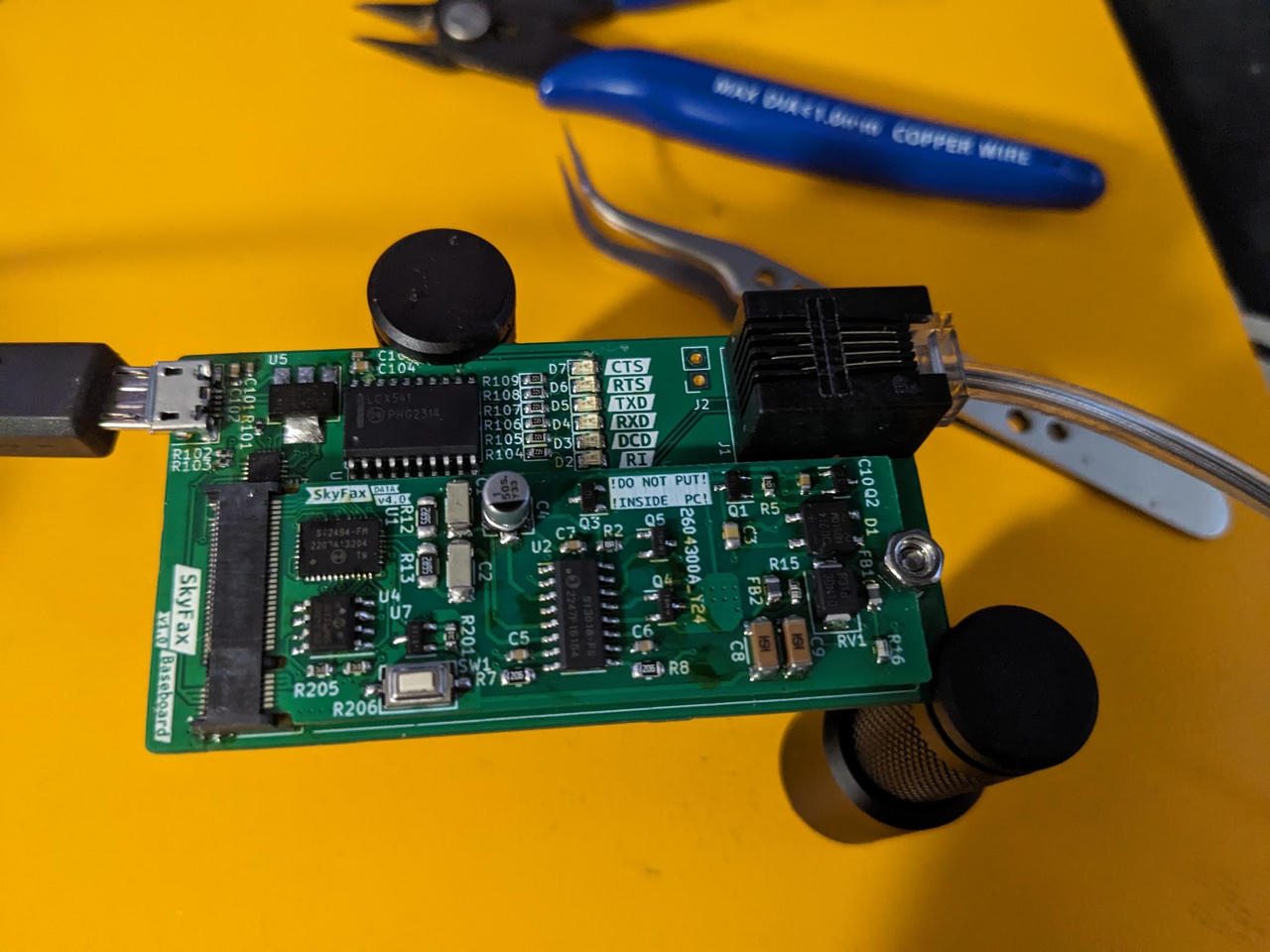
For the shape and size, not only did I want it pretty compact, I wanted it to be on a module, since the modem was supposed to be part of another bigger project. I split out the CP2102 UART chip and the RJ11 connector onto an adapter board, and the main modem module just contain the modem circuits, with the system-side exposing UART signals and line-side exposing the telephone wires. While looking for good board connectors, I thought of the M.2 connectors usually found on SSD or NVME drives. Turns out, these are actually called NGFF (Next Generation Form Factor)5 connectors, and have a couple different keying interfaces (different notch locations and pin count).
I liked the idea of using the M.2/NGFF connectors, and it would work for my case since I only need a few signals (power, ground, telephone side tip&ring, 8-ish UART serial signals) to connect to the USB adapter board.
It would have been annoying to try to rewire and match the M.2 pinout to be compatible with computer M.2 ports (especially within that small constrained area), so I just made up my own convenient pinout and put a warning label saying, "!!! DO NOT PUT INSIDE PC!!!".
Regarding the layout of the components, once again, the application note3 was VERY helpful, especially Section 4.4: Layout Guidelines. Again, I followed the guideline and the reference placement (roughly) and hoped for the best.
Add some test points to traces where you think might be useful later while debugging. Jumpers and clippable jumpers are also useful too, in cases where it'd be very difficult/annoying to solder and desolder components during testing. For example, I added some jumpers (with labels) on the UART signals, so that (1) I can test the UART bridge and (2) use a separate UART adapter instead if my designs were incorrect.
KiCAD
The steps for PCB layout are a bit similar to those for schematics above:
- Lay out the components roughly where they'll be. The white line shows what should be connected to what, so move and rotate things accordingly.
- Start laying out traces, moving components as needed.
It helps to work on different "subsystems" at a time. For example, lay out the components and traces for voltage regulator circuit, and then group it together so that they move together as one and the relative position is fixed. - Repeat last step?
- Do until satisfied.
- Move / resize / hide designators and value labels as needed.
- Create board edge and ground fill.
I really like the KiBuzzard plugin.
It lets me create very nice labels.
Try it.
Optionally, you can assign 3D models. KiCAD has a built-in 3D render viewer6. If KiCAD's default libraries do not have a model for your components, you may have to source the 3D models online (either another KiCAD library or step/wrl file) or draw one yourself.
PCB Fabrication
Sometimes, for simpler projects or prototypes I don't want to wait for, I make the boards at home, which takes a few hours compared to a few days + shipping. See my other post describing the process.
Usually though, if I have more time and don't mind waiting, I send off the design to a fab where they'll make the pretty boards, with soldermask and everything. I usually go to JLCPCB because they are pretty cheap, and since their (expanding) capabilities are enough for most of my projects. There are other fabs too; many in the US as well.
But before I produce the manufacturing files, I need to ensure that design constraints are met and also that the manufacturer (in this case, JLCPCB) can actually produce it (trace gaps, trace width, minimum tolerances, etc). In KiCAD, you can enter design rule constraints (both electrical and board) and run checks. You can find the fab's capabilities on their site. For JLC: here.
Once that's all done and rule checks are passing, I can export the gerbers and upload.
Check out Fabrication Toolkit and KiCAD JLCPCB Tools plugins. They make exporting to JLCPCB a bit easier by generating a zip you can upload, instead of individual gerbers.
Assembly
After I've uploaded and JLCPCB has verified my design, it will go into production. I've also ordered the components at the same time.
After waiting a week or so, I have the boards in my hands, and all the components I need to populate it. So I get to soldering.
The Interactive BOM is a plugin you should definitely install and use. It generates nice interactive HTML page with all the components in a table and a board view. It'll save a bunch of time trying to find which component goes where and figuring out which components have been placed already.
You can also have the boards fully assembled for you. Many PCB manufacturers now offer assembly services for cheap. I haven't tried JLC's service (I actually like to sit at my lab bench, put on some music, and solder things one by one), but I hear it's okay for simpler projects.
If you order the assembly service from JLC, the steps are pretty similar to how I added the DIGIKEY field in the BoM. You just specify the part number from JLC's component library and when ordering the PCB, add on the assembly service.
I soldered the USB UART chip (CP2102) first, along with all the components to power and operate it (resistors, connectors, etc), since it's the easiest to test.
Connect the RX and the TX pin together, and type things into minicom(1)7 (see below for basic tests using minicom).
If it's working properly, whatever I typed should go out to TX, back into RX, and show up on the screen.
Next, the main modem chip (Si2494) and its supporting components.
We can't do any real modem stuff yet since the line side is not populated.
Connect it back up to minicom and type in AT<enter>. If it responds OK, then it is working correctly.
I can now finish up the rest of the board and fully test the modem.
The version 2 did not have its own UART bridge, so I used the evaluation board. After everything was soldered, I replaced the modem module with the one I built. Here's a screenshot of a video I took while testing the version 2:
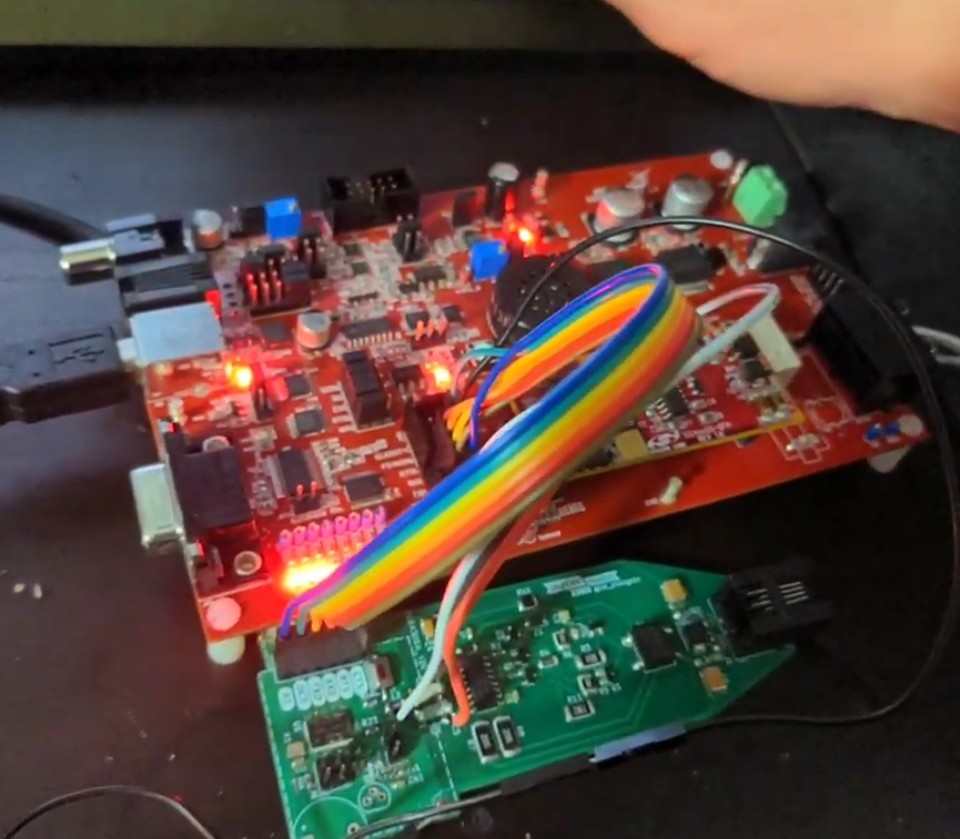
It didnt work immediately, so I disconnected the capacitors between the system and line sides on my module and the reference module. I tested my system side with the reference line-side circuit and vice-versa. This was a while ago, so I don't quite remember what was wrong.
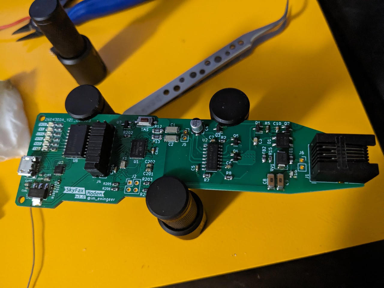
After that, I drafted up version 3, sent it over to the fab, and repeated the process. You can see below that the version 3 (the long one) has a row of jumpers (J4) near the modem chip (U1) towards the left side. That allowed me to easily probe and also disconnect the UART circuit so I could use a different, working, UART USB bridge (or the evaluation board) for testing.
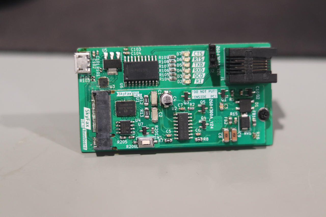
Version 4 separated out the adapter board and the modem circuits. Here are some pictures of the v3 and v4 module after being assembled:
Final Build
Once everything was put together, it came out to look like this:
I also had some time and was bored, so I designed a case for it:
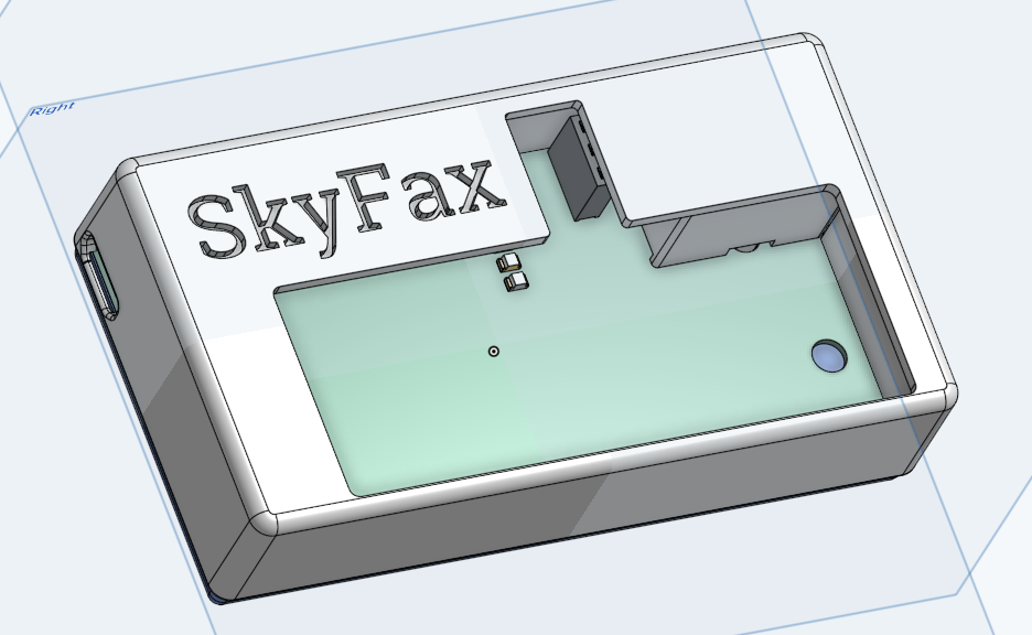
The 3D model of the modem module + USB adapter board was exported from KiCAD and imported into OnShape, giving me reference shapes and dimensions to design around. It was then 3D printed. The text part was extruded inwards to create a "well" where it can be filled with some polyurethane resin.

Using the Modem
I do not have an active landline at my place (although now, I have set up an internal retro network).
Luckily, I do have an old telephone line simulator.
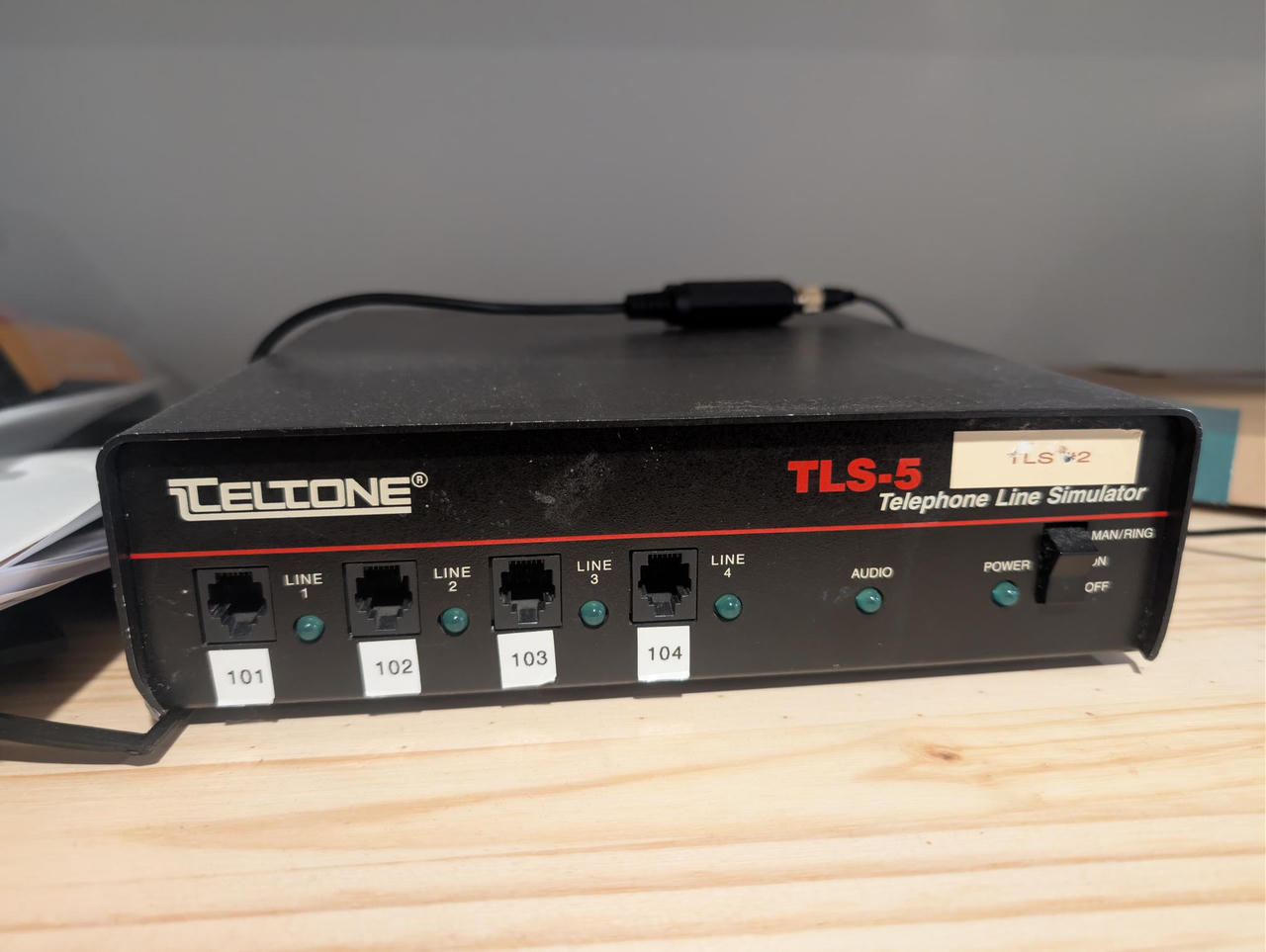
You can connect phones and devices to the different ports and dial each other with the numbers written on them. So after building two of the modems, connecting them to 101 and 102, I hooked them both up to my machine and opened up the serial terminal using minicom(1)7.
You can test if the communications to the modems are working by sending a blank AT command, and (1) you should see what you type echo'd back to you, (2) the modem should respond with a single OK. If this does not work, check the serial port settings (baud rate, stop bits + parity, and also see which combination of hardware/software flow control works).
Here, the left side is the modem connected to 101, and the right 102.
It's hard to see the text on the screen due to my camera not being focused properly. Enable captions to show the commands I typed. I am using the audio output of the telephone line simulator, so the audio is heard continuously.
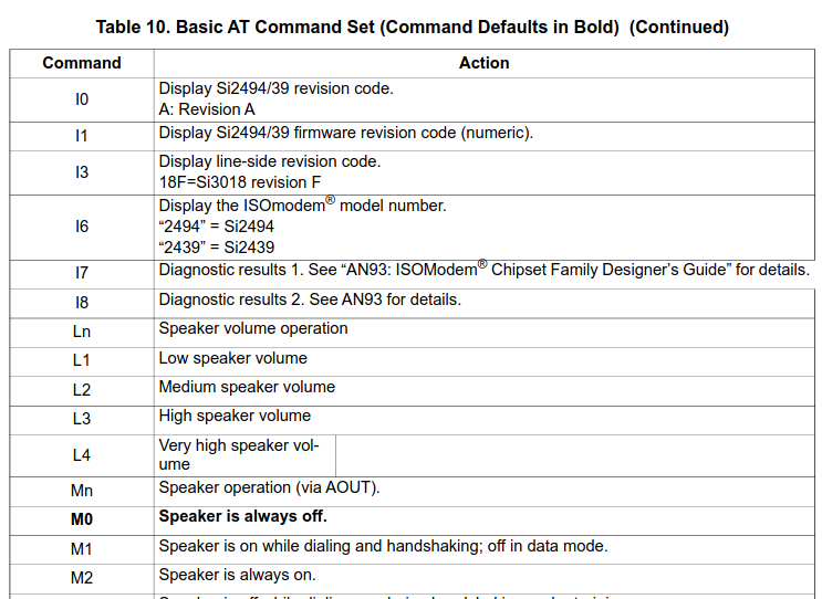
The modem can be configured using AT commands listed in Tables 10 and 11 of the datasheet, as well as the AN933.
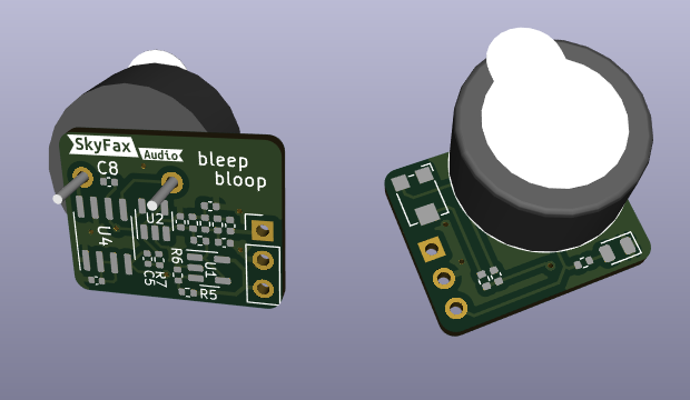
Audio Module
Version 3 adds a header for an optional audio module. There are also schematics and PCB layout for this in the project files, under SoundCard/.
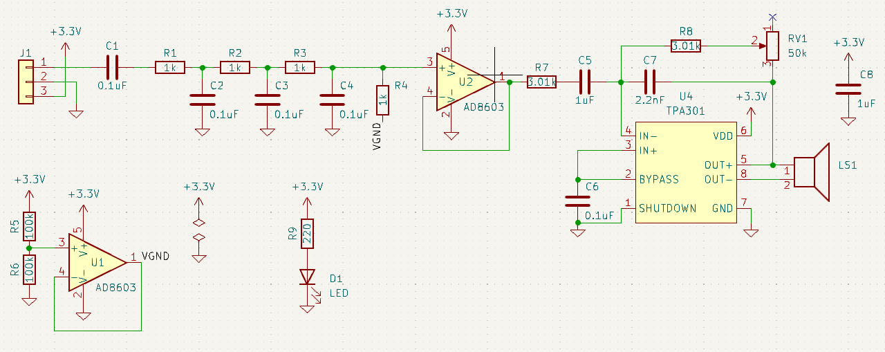
By default, the modem won't produce any sounds, even with the audio module plugged in.
Use the command ATM1 to enable sounds during handshake, ATM2 for audio always on like in the video above using the line simulator.
Without a Line Simulator
If you don't have a working landline nor a line simulator, you can connect two modems using this simple circuit instead8:
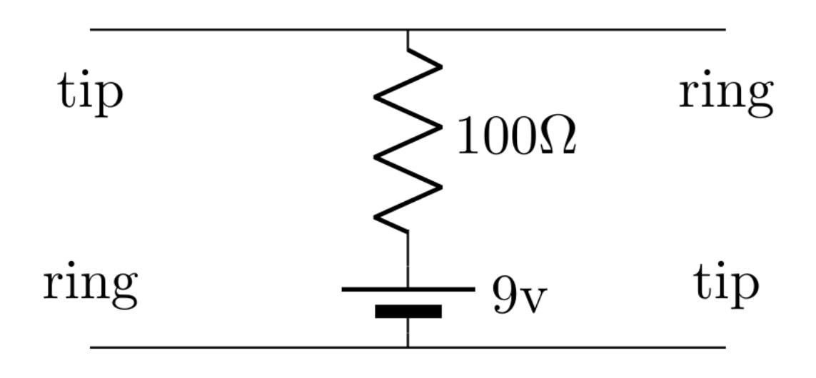
There are other variations of this circuit available online, but I found this one to work for me and this setup. The voltage and resistance can be tweaked to provide ~20mA of current with the modem/phone off-hook.
There are also schematics and PCB layout for this in the project files, under LineSim/.
This circuit, however, will not produce a dial tone, so dialtone detection must be disabled with ATX3 command. Then you can dial with ATDT on one modem and answer with ATA on the other.
Fax?
Oh, I finished the project and was really excited to test the dial-up (data) mode, which worked.
But going back to the original purpose, which was to provide fax capabilities to an electronic badge, I found that this chip (the Si2494) does not support fax mode...
There was another chip that was compatible (like, just drop-in replacement) that did support fax mode, but going back on DigiKey and looking for it, it seems like it wasn't actively being maufactured nor in stock anywhere.
Well, no fax for this module I guess.
Cheers
73,
-B
-
A Low-Dropout Regulator (LDO) is a linear voltage regulator that maintains a stable output voltage even when the input voltage is very close to the desired output. ↩
-
Skyworks Application Note 93 Si2493/57/34/15/04 (Revisions D and D1) and Si2494/39 (Revisions A and A1) Modem Designer’s Guide ↩ ↩2 ↩3 ↩4
-
KiCAD is an open-source PCB design and electronics CAD software. I really like it and in the recent couple of years, has gotten really good and is even starting to catch up on features previously only available to those on paid, commercial software. ↩
-
https://en.wikipedia.org/wiki/NGFF (redirects to M.2) ↩
-
I found this and that resources to be helpful to connect two modems together without a proper telephone line. ↩